10+ stm32 block diagram
Here are the STM32 MAX7219 dot matrix connection diagrams for single unit display two independent slave units and finally two or. After uploading the code open Serial.

Stm32f042k6t6 Microcontroller Datasheet Nucleo Schematic Video Faq
Above block diagrams are self explanatory.

. All the STM32 general-purpose timer peripherals share the same backbone structure. Bind the Block to server address and port. How to do Firmware Update over the Air FUOTA for B.
555 Timer Circuits Op-amp Circuits Audio Circuits Power Supply Circuits Arduino Projects Raspberry Pi Projects MSP430 Projects STM32 Projects ESP8266 Projects PIC. Perform the above discussed problem on a third order differential equation. We have used an Arduino Nano for controlling whole this Metal Detector Project.
Five-volt tolerant abbreviated as FT The equivalent GPIO diagram structure for TT or FT is given in Figure 2. ESP32 Getting Started with Deta Base Unlimited and Free Database for Developers. STM32 MAX7219 Dot Matrix Display Module Connection Diagram.
The 555 timer is used to generate a PWM signal with. A Coil and capacitor is used for the detection of metals. STM32 Blue Pill UART Interrupt with CubeIDE and HAL Libraries.
With an 36 MHz ADC clock it can achieve 24 mega samples per. Offline uninterruptible power supply block diagram. Receive Data In RX and Transmit Data Out TX.
And here is the functional block diagram for the internal structure of the MAX7219 driver IC. A LED and Buzzer are used as metal detection indicator. The ADC needs a minimum of 3 clock cycles for the sampling and 12 clock cycles for the conversion.
Any USART bidirectional communication requires a minimum of two pins. And a resistor for limiting the current to the Arduino pin. The following image depicts the block diagram of the PWM based LED Dimmer using 555 Timer IC.
USART Baud Rate Settings STM32 Cortex M3. Three-volt compliant abbreviated as TC. Here is the complete circuit diagram for cell phone.
After the simulation is complete double click on the scope and the waveform of the equation is displayed as shown in the figure below Figure 23. The equivalent GPIO diagram structure is given in Figure 1. Running the block diagram.
This section tears down the advanced configuration TIM1 timer peripheral which is the timer peripheral with the most features. Listen for the incoming requests by the client 4. Run the block diagram from the Run icon as shown in the figure below Figure 22.
One input and meny outputsbut output current will be different. Followings are the basics difference between them. So you can see where the SPI data we send to it goes.
First we need to do the circuit connections as shown above in the circuit diagram. Three-volt tolerant abbreviated as TT. Offline UPS block diagram.
STM32 USART Hardware Functionalities In this section well get a deep insight into the STM32 USART module hardware its block diagram functionalities BRG modes of operations and data receptiontransmission. A signal diode is also used for reducing the voltage. STM32 products integrate three main GPIO basic structures.
Figure 1 shows the block diagram for. ADC in STM32 The. I need block daigram and circuit daigram power supply.
A 12V DC source is used to power the entire circuit including the 555 timer IC and the LEDs. The analog-to-digital converters inside STM32 products allow the microcontroller to accept an analog signal like a sensor output and convert the signal into the digital.

Stm32f042k6t6 Microcontroller Datasheet Nucleo Schematic Video Faq
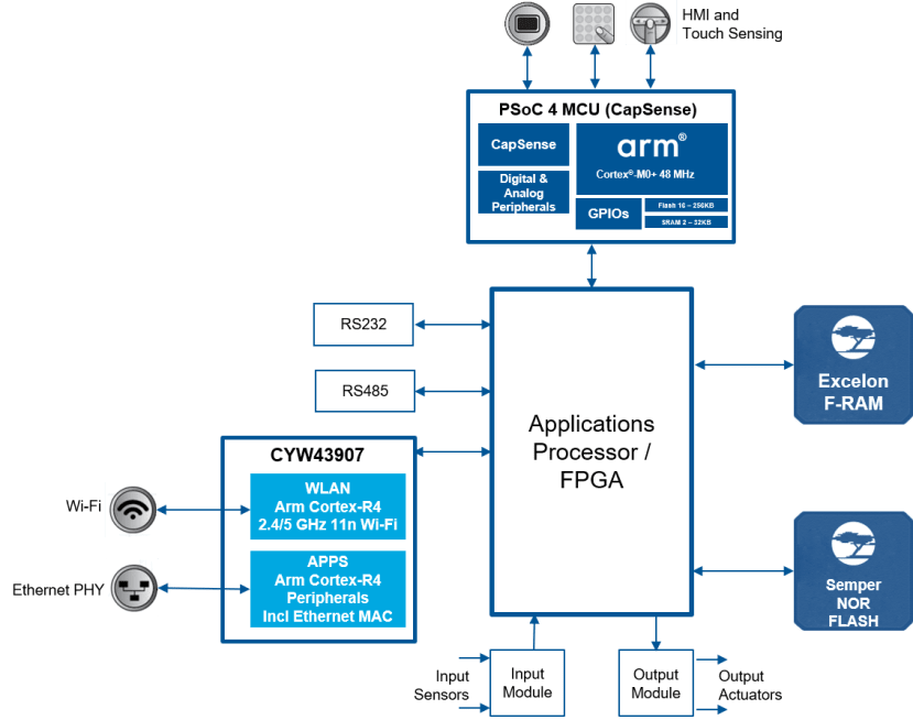
Programmable Logic Control Plc Solution From Cypress Semiconductor

Schematic Diagram Of The Control Stage Download Scientific Diagram

Motorola 68hc11 Wikiwand

Stm32f407vet6 Microcontrollers Cad Models Datasheet Features Video Faq

Implementing A Two Axis Robot Arm Controller Without An Mcu Edn Asia
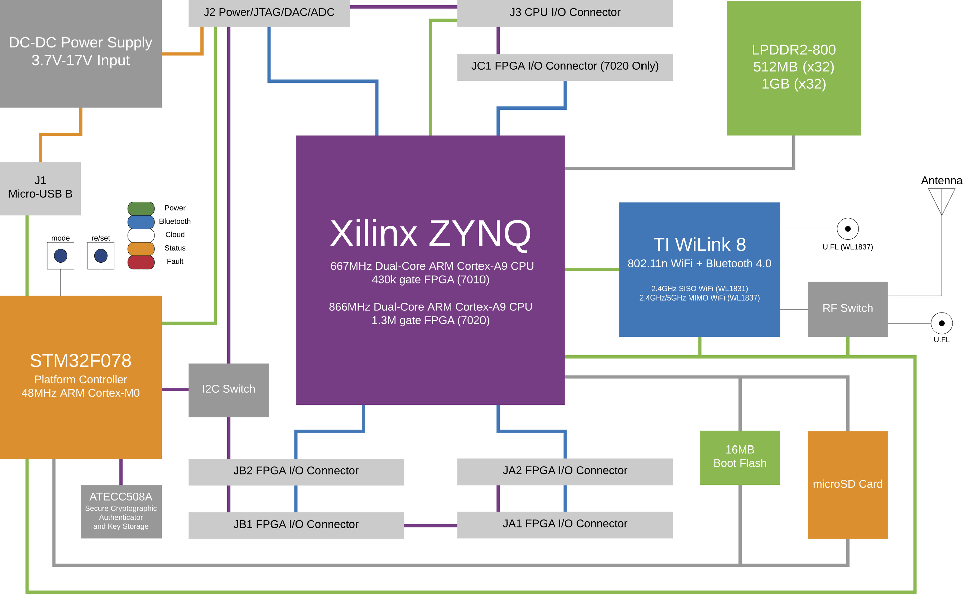
Snickerdoodle Xilinx Zynq Arm Fpga Board Starts At 55 Crowdfunding Cnx Software
Stm32f030c8t6 Microcontroller Datasheet Pinout Programming Manual Video Faq

Stm32f429zit6 Microcontroller Datasheet Reference Manual Pinout Faq
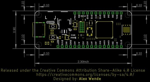
Sparkfun Thing Plus Stm32 Dev 17712 Sparkfun Electronics

Stm32f4 Discovery Board Pinout Configuration Features And Examples Analog To Digital Converter Discovery Output Device

Pin Diagram Of Stm32 Discovery Board Pic Microcontroller Microcontrollers Gaming Console

Stm32f042k6t6 Microcontroller Datasheet Nucleo Schematic Video Faq
What Is The Block Diagram Of Usart 8251 Quora

Schematic Diagram Of The Control Stage Download Scientific Diagram
What Is The Block Diagram Of Usart 8251 Quora
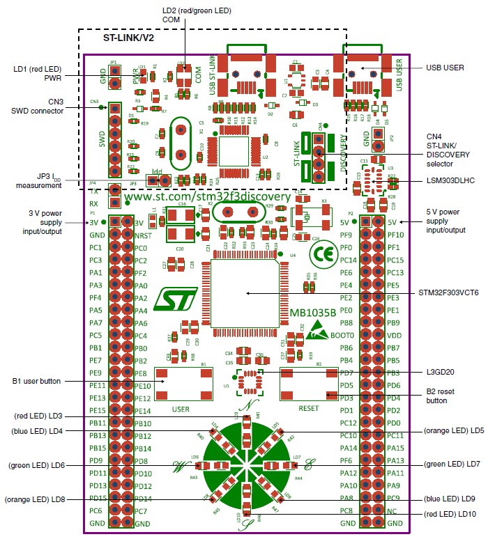
Blink The Leds Of Stm32f3 Discovery Board Part 2 Knoldus Blogs